
Another nice feature from Microchip microcontrollers is CLC – Configurable Logic Cell. It have logic gates and latches, that we can configure to create some logic circuits with inputs and outputs from microcontroller pins or internal signals.
That functionality could be made internally inside program, but then the limitation would be the system clock. The great thing is that CLC works independently from microcontroller core, so the input and output don’t have to be synchronized with internal clock. It should work faster, and also microcontroller core is free to do something else.
The main parameter that defines the speed of logic is propagation delay. Propagation delay is delay between signal change on circuit input (rising or falling edge of signal), and signal change at output (caused by that input change). Of course signal cannot change in infinitely short time, so usually the time of signal change is defined as time when the signal crosses the midpoint between low and high steady state.
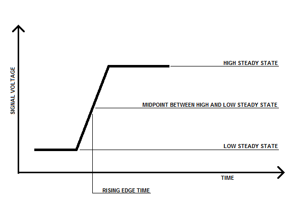
So if the logic works that rising edge on input causing rising edge on output, then the propagation delay is defined as the time between midpoint of rising edge on input and midpoint of rising edge on output. Sometimes in logic circuits there are two different propagation delays for single input – propagation delay on rising edge on input and propagation delay on falling edge on input. If the logic circuits have many different inputs, then also propagation delay can be different on each input.
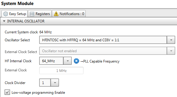
In this article I would like to measure the propagation delay of CLC in various configurations, because I couldn’t find that information in datasheets. The measurements will be made on new MPLAB Xpress PIC18F25K42 board.
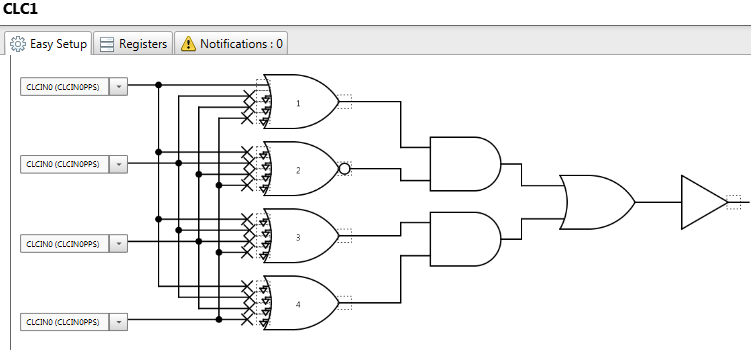
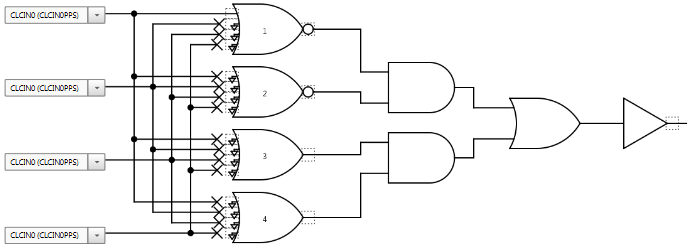
 Great thanks to Microchip for sending me that board for tests. The possible logic cell configurations are showed on image below.
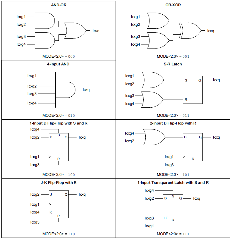 This picture is taken from PIC18F25K42 microcontroller datasheet. The logic inputs Icxg1 … Icxg4 can be connected to external pins of microcontroller or to output of any internal peripheral of microcontroller (or at least a lot of peripherals.. i didn’t checked it). All signal on inputs can be connected directly or can be negated. Output of logic cells also can be connected to external pins of microcontroller or input of internal peripherals and also can be negated. In that test I will connect inputs and outputs to pins of microcontroller, so I could measure the time difference on inputs and outputs.
I need some signal source that I could connect to logic inputs. For that purpose I could use some externall generator, but it will be easier to to use one of microcontroller peripherals – Timer 0. The output of that timer will be connected to some other pin and I will connect externally that pin to logic input pin of our CLC. Actually I could connect that timer output to input of CLC just by configuring it properly, but I’m interested in propagation delay including the delay on pin input buffers. If I connect it internally I will probably bypass that buffers. As usual I’m using Microchip Code Configurator – tool which saves me a lot of time.
System configuration is showed on picture below.
 TIM0 is set up to generate signal which period is 40 ms (20 ms low state and 20 ms high state).
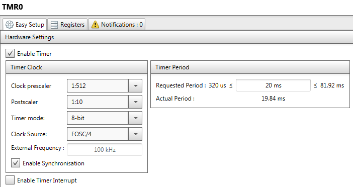 First I will test the CLC in AND-OR configuration, which is simplest to test.
 As you can see on the picture, the logic circuit is very simple. It copies the input signal to output without any changes. The second OR gate (on the left) have negated output to force it to 1, because otherwise the AND gate would have always 0 on output.
On the picture below there is configuration of output pins.
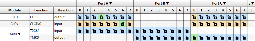 The TMR0 output is connected to port C pin 0. First input of logic cell (CLCIN0) is connected to port A pin 6, and output of CLC1 is connected to port A pin 3. I made external connection between pin C0 and A6 (on the board those pins are next to each other), so output of TIM0 is connected to CLC input.
I had to make small modification in main.c file, to make output slew rate of microcontroller pins as high as possible (shortest rising and falling edges on outputs).
void main(void)
{
    SYSTEM_Initialize();

    SLRCONA = 0x00;
    SLRCONC = 0x00;
    while (1)
    {
    }
}
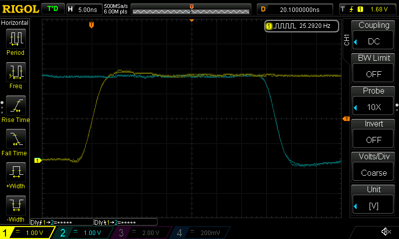
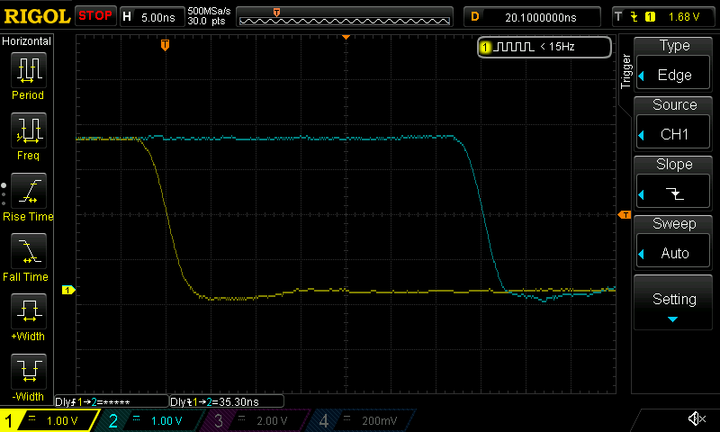
Now we can turn on our board and connect oscilloscope probes to pins C0 (or A6) and A3. The rising and falling edge propagation delay is showed below.
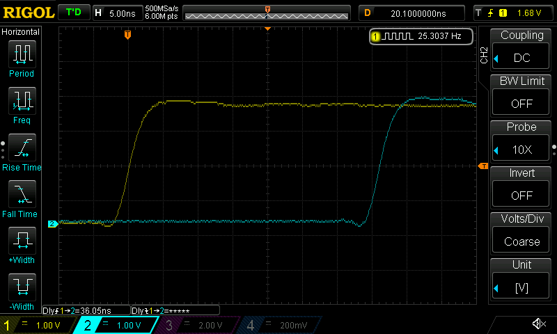
 The yellow signal is input, and light blue is output. As you can see, the propagation delay in both cases on OR-AND configuration is about 36 ns.
Now lets change output of OR gate to negative.
 Input and output signal now looks like that:
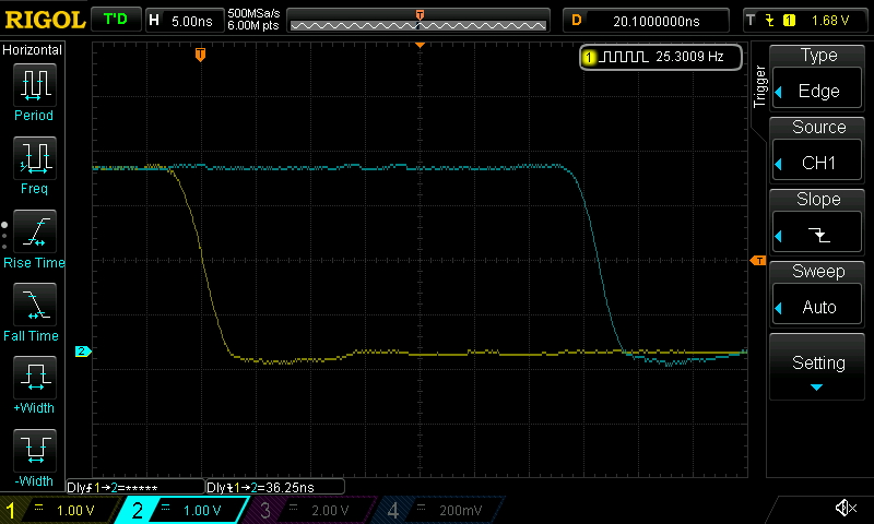
 Propagation delay in that case is about 1 ns longer, but in comparison to total propagation delay it’s not much difference. Lets check the falling edge propagation delay:
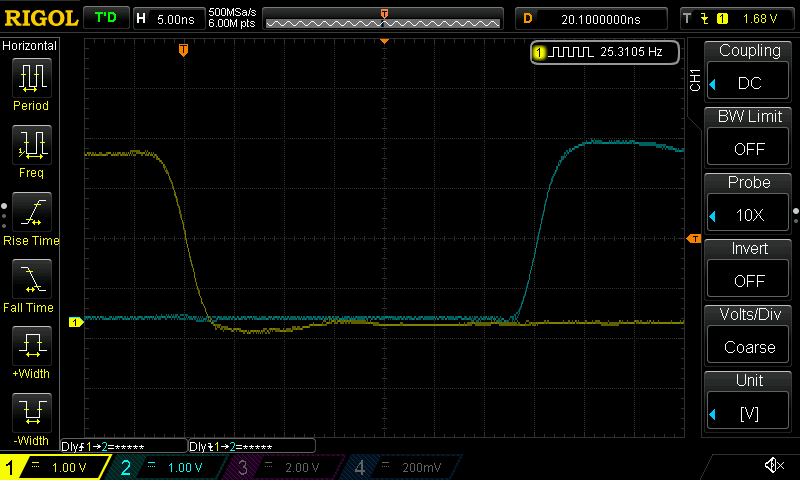 Well now the delay is 1 ns shorter. But anyway there is always really close to 36 ns.
I made a lot of other measurements, and I show here just few of them. This is JK flip-flop configuration with J and K signal equals 1, and clock signal is negated. In that configuration when the clock signal have falling edge, then output of flip flop changes state to opposite.
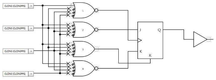 On oscilloscope we have the case when output changes from 1 to 0 (but in that configuration, next falling edge will change output from 0 to 1).
 The propagation delay is about 36 ns again (well, actually 35 ns).
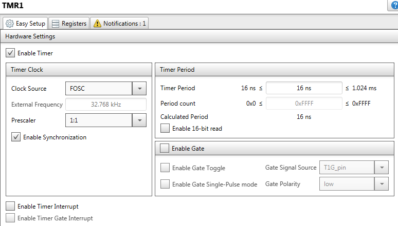
Now lets test some more complicated case. Lets test propagation delay from RESET pin to output. When reset pin is High, then the output should be set to low. But to test it we should somehow set the output to 1. To make it happen, we’ll modify our project. To set output of flip flop to 1 in period of 1 ms we’ll set inputs to J = 1 and K = 0 and generate signal on clock input. As clock signal on clock input of our JK flip flop, we’ll use timer 1:
New configuration of CLC:
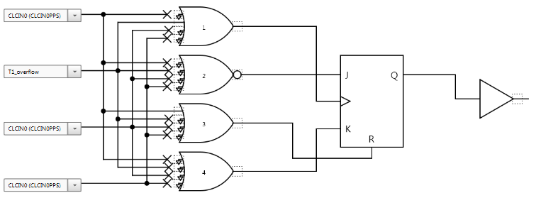 Now our input signal is connected to R input of JK flip-flop (the 40 ms clock signal), and output of timer 1 (T1_overflow, which is 2 ms clock signal) is connected to clock input of flip flop. The J=1, K=0 so the rising edge on clock signal will set output of flip-flop to 1 in period of 2 ms. The R input have higher priority, so when we have rising edge of R pin the output will change to 0 (regardless of other inputs). In that configuration we are forcing output to be high every 2 ms, and every 40 ms we are resetting output to low by setting R pin high.
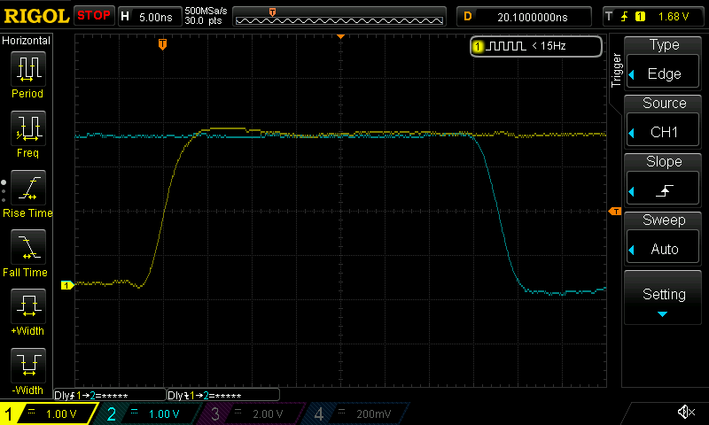 The propagation delay is about 38 ns.
Conclusion
Propagation delay of CLC is about 36 ns (35 – 38 ns). The great thing is that propagation delay is quite similar in all configurations of CLC and it’s the same on falling and rising edge of input signal.
That peripheral is useful to make some logic outside microcontrollers core, so microcontroller can do some other stuff in the same time.
Doing that logic in microcontrollers core will probably take all it’s time just to check inputs and sets outputs continuously, and also it would work much slower. Also the output would be correlated with system clock, not just the input signals, so reaction time would be different each time the input signal changes.
Once again thanks to Microchip for that test board.